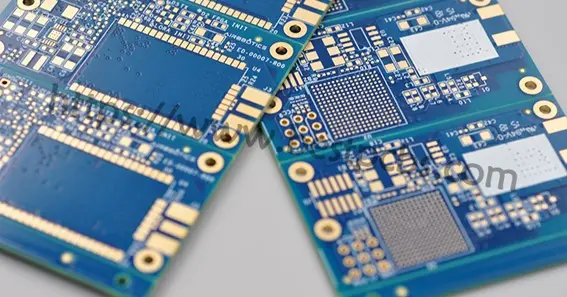
In PCB (Printed Circuit Board) design, one of the essential features is the application of a solder mask to control where solder can adhere. A gang-mask shape around the pin field is a strategic design choice that involves creating a single, contiguous solder mask opening around a cluster of pins or pads on a PCB. This technique can significantly impact soldering quality, reduce defects, and enhance the overall reliability of the board.
What is a Gang-Mask Shape?
A gang-mask shape refers to a unified opening in the solder mask layer that covers multiple pads or pins at once, as opposed to having individual openings for each pin. This approach is particularly beneficial for densely packed components like BGAs (Ball Grid Arrays) or connectors where solder bridging and thermal management are critical concerns.
Also Read N: Should You Buy A Ford Mach-E Lemon? Here’s What You Need To Know
Benefits of a Gang-Mask Shape
- Reduced Solder Bridging: The gang-mask technique minimizes the chances of unwanted solder bridges between adjacent pins, which can cause short circuits. It ensures that solder is confined precisely to the designated areas.
- Improved Manufacturing Precision: By combining multiple openings into a single mask, manufacturers can achieve higher precision, particularly in cases where traditional masking might result in misalignment due to board warping or slight inaccuracies in the photolithography process.
- Enhanced Heat Dissipation: In high-power applications, a gang-mask shape allows better thermal dissipation, as the larger exposed area helps to dissipate heat more efficiently compared to smaller, individual openings.
Also Read P: Charter Bus For Summer Camp: A Smart Transportation Choice
Key Considerations for Designing a Gang-Mask Shape
- Clearance Requirements: Ensure appropriate clearances are maintained between the mask opening and the pins to avoid solder mask encroachment, which can lead to improper solder joints. A common recommendation is to maintain a 75–125 µm gap around each pin to allow proper solder flow.
- Manufacturing Compatibility: Different PCB manufacturers might have specific standards for gang-mask designs. It is crucial to check whether your manufacturer supports this technique and if they require any particular adjustments during the design phase.
- Material Selection: The type of solder mask material (liquid or dry film) can affect the quality of a gang-mask opening. Liquid photoimageable masks are often preferred due to their ability to produce high-resolution patterns and tightly controlled tolerances.
Common Applications of Gang-Mask Shapes
- BGA Components: BGAs are one of the primary applications where gang-masking is beneficial, as it provides a clean opening that covers multiple solder balls while reducing the risk of solder defects.
- Connectors and Dense Pin Fields: When multiple pins are closely packed, a gang-mask design simplifies the soldering process and enhances the reliability of solder joints, ensuring better electrical conductivity.
FAQ
- What is the purpose of a gang-mask shape in PCB design?
- A gang-mask shape is used to control solder application across multiple pins or pads simultaneously, reducing solder defects and improving manufacturing precision.
- How does a gang-mask shape prevent solder bridging?
- By creating a single unified mask opening, a gang-mask shape minimizes the chance of solder accidentally bridging between closely spaced pins, avoiding potential short circuits.
- Which components benefit the most from gang-mask designs?
- BGAs, connectors, and other densely packed components benefit from gang-mask designs due to improved soldering quality and reduced assembly errors.
- What materials are suitable for creating a gang-mask shape?
- Liquid photoimageable solder masks are commonly used because they allow for high precision and fine detailing necessary for complex patterns like gang-mask shapes.
- What clearance is recommended for gang-mask openings?
- A typical clearance range is 75–125 µm around each pin to ensure proper soldering and mask application without encroachment.


